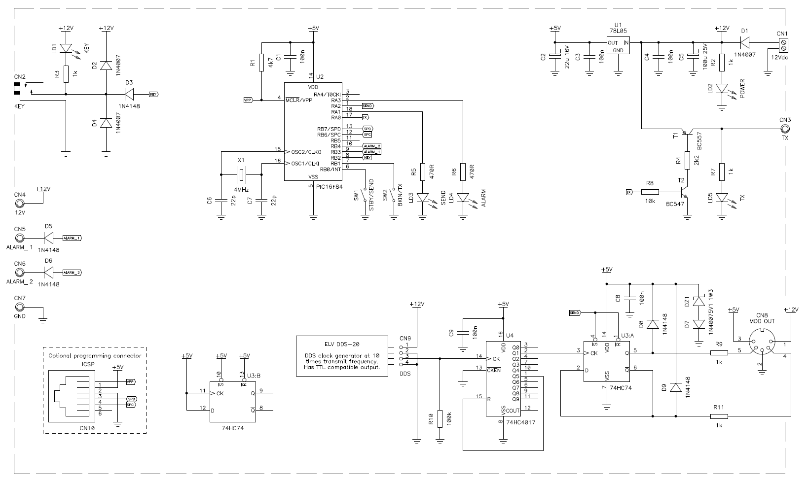
Circuit diagram of the driver unit (click to enlarge). – A PDF version is also available: drivercircuit.pdf (49,011 bytes).
The driver unit is the control center of the whole transmitter. It generates the CW "modulation", handles alarms, handles break-in timing and generates the desired carrier frequency.
As for every transmitter, first we need a VFO. The VFO runs at ten times the output frequency, meaning form 1.357 to 1.378 MHz for the 137 kHz band and probably around 5 MHz for the 500 kHz band. Here a DDS kit ELV (named DDS-20) was chosen, first because of its price, but also because it already has a TTL compatible output. This DDS can be programmed to work with a PLL multiplier, but unfortunately not a ÷10 frequency divider as in our case. To make things simple, a multiplication factor of 100 has been programmed (referring to its operating manual) so that the frequency displayed is actually 1000 times higher than the desired transmit frequency and one just has to know that the display says "MHz" but it actually means "kHz".
Any oscillator can be made to work by slightly modifying the circuit to adapt its output signal to TTL levels, but LC based VFO circuits should be discarded because of their poor frequency stability: when operating in QRSS, a frequency drift of only a few Hz could be catastrophic. Any DDS will do the job, but other frequency synthesizers will work as well. Other ideas for a VFO are good (stable) laboratory frequency generators or even the station HF transceiver.
Circuit diagram of the driver unit (click to enlarge). –
A PDF version is also available: drivercircuit.pdf (49,011 bytes).
So a TTL compatible signal at 10 times the output frequency is applied to CN9 and goes into U4, a classical 74HC4017 Johnson counter. This will divide it by 5, providing an asymmetric signal at twice the carrier frequency on pin 2. This drives the clock input of U3:A, a D-type 74HC74 flip-flop, that will divide it by 2 generating two complementary and symmetrical signals at the desired carrier frequency. U3:A is controlled by the "SEND" signal applied on its pins 1 and 4: when this signal is high it operates normally generating the carrier signal; when it goes low both outputs will go high cutting off the RF. D7, D8, D9, DZ1, R9 and R11 protects U3 when things go terribly wrong in the final unit, but still, mounting U3 on a socket is a good idea. R10 just pulls down the clock input of U4 in the case the DDS is disconnected. U3:B is not used. So, two complementary and symmetric TTL signals, CW manipulated will drive the final unit through CN8. LD3 just follows and shows the status of the "SEND" signal.
The two complementary outputs can be observed in the figure below (for the first 10 μs, the flip-flop is blocked and than start generating the carrier at about 0 μs):
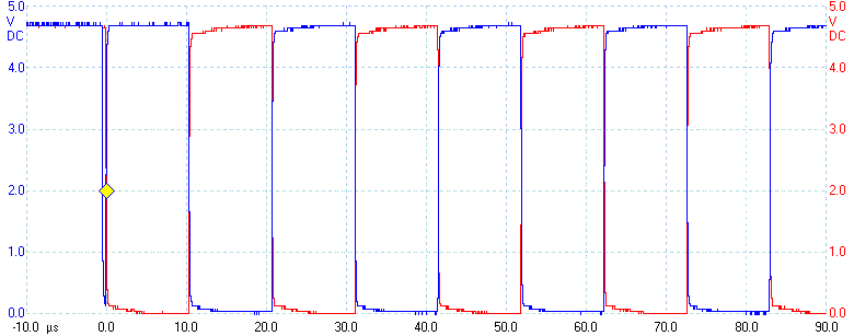
Driver outputs on keydown.
The CW key connected to CN2 cannot be directly used to manipulate the RF amplifier since the antenna has to be switched first from the receiver to the transmitter. This is done in the TX/RX switch unit by a relay and takes some time. Appling the RF too early will result in arcing between relay contacts and the MOSFET transistors of the final unit may blow up. Measures show that the relay switch time is about 9 ms: to be on the safe side, this unit will wait 12.3 ms before applying RF to the final unit.
This delay can be observed in the figure below, where the red trace is the CW key and the blue trace is one of the two outputs:
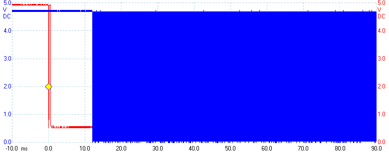
TX delay on key-down.
The CW key is connected to CN2. R3 and LD1 act both as pull-up and as monitor to check the wiring of the key (useful for preventing unwanted transmissions when checking the wiring). D2, D3 and D4 protect the microcontroller against "bad" voltages on CN2.
The first version of this unit used C-MOS gates and RC networks to generate all the timings, but it was too complicated and not flexible enough. It was therefore redesigned replacing all the logic gates with PIC16F84 microcontroller and all the timings are now implemented in software by a state machine. The PIC16F84 is easy to program and, since it's getting pretty old, one usually has a lot of those in the junk box... It has been programmed in C, using HI-TECH PICC compiler; the free version is enough. If one wants to recompile it with a different tool, please remark that for PICC, an "int" variable is only 16 bit and not 32 as usual.
The firmware to program the PIC is available here: lwdriverunit.zip (5,758 bytes).
The archive contains the compiled .hex file that can be directly programmed into a PIC16F84 and the C source code to allow modifications.
The control unit has two switches: SW1 ("Send/Receive") and SW2 ("Break-in/TX"). If SW1 is open the transmitter is disabled, the antenna is connected to the receiver and the status of the CW key is ignored. When SW1 is connected to ground, transmission is enabled. Now, if SW2 is open, when transmitting, the antenna is immediately connected to the transmitter and stays there as long as SW1 is grounded; manipulating the key will, of course, apply RF to the antenna. If SW2 is grounded (break-in mode), the transmitter will automatically switch between TX and RX following the CW key. The delay before returning back to receive mode has been set to 1 s, but this can be easily reduced to something like 10 ms in order achieve full break-in (QSK) operation: you just need to modify the corresponding constant and recompile the software.
Alarms lines are connected to CN5 and CN6. Diodes D5 and D6 protect U2 inputs from over voltages. Internal weak pull-ups in U2 are used. If one of these lines goes high the RF is immediately switched off and the microcontroller will display the alarm on LD4. It will switch on LD4 continuously if the problem came from CN5 or it will blink LD4 if the problem came from CN6. To recover from an alarm condition, just open SW1.
At startup, an initial delay of 0.5 s allows all voltages to set before starting the transmitter, than a safety check is done preventing transmission if the "Send/Receive switch SW1 was forgotten in the "transmit" position (LD3 will blink until SW1 is opened).
All the logic circuits of this unit are powered by a 5 V supply regulated by U1. Transistors T1 and T2 are used to provide the necessary 12 V supply to the antenna relay on the TX/RX switch unit when transmitting. LD5 informs about the status of the transmitter.
The optional ICSP connector was planned for reprogramming the microcontroller without removing it from the circuit, but finally it was not installed.
The following pictures just show the inside of this unit:
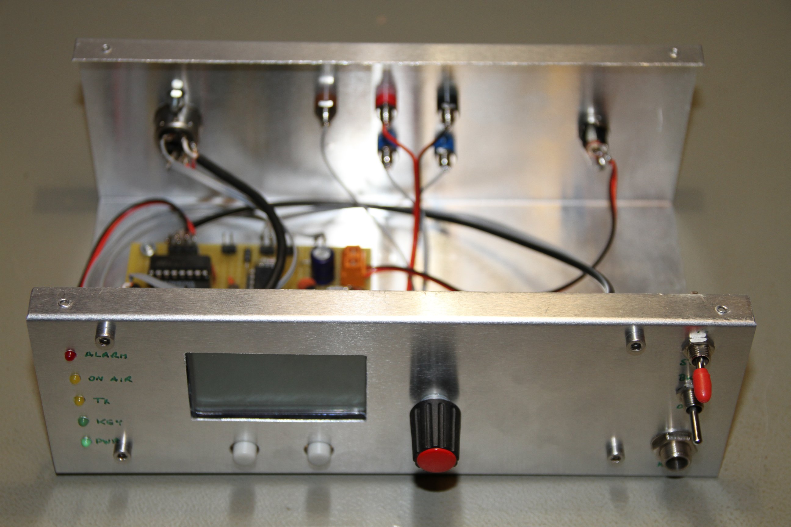
Driver unit, front view (click to enlarge).
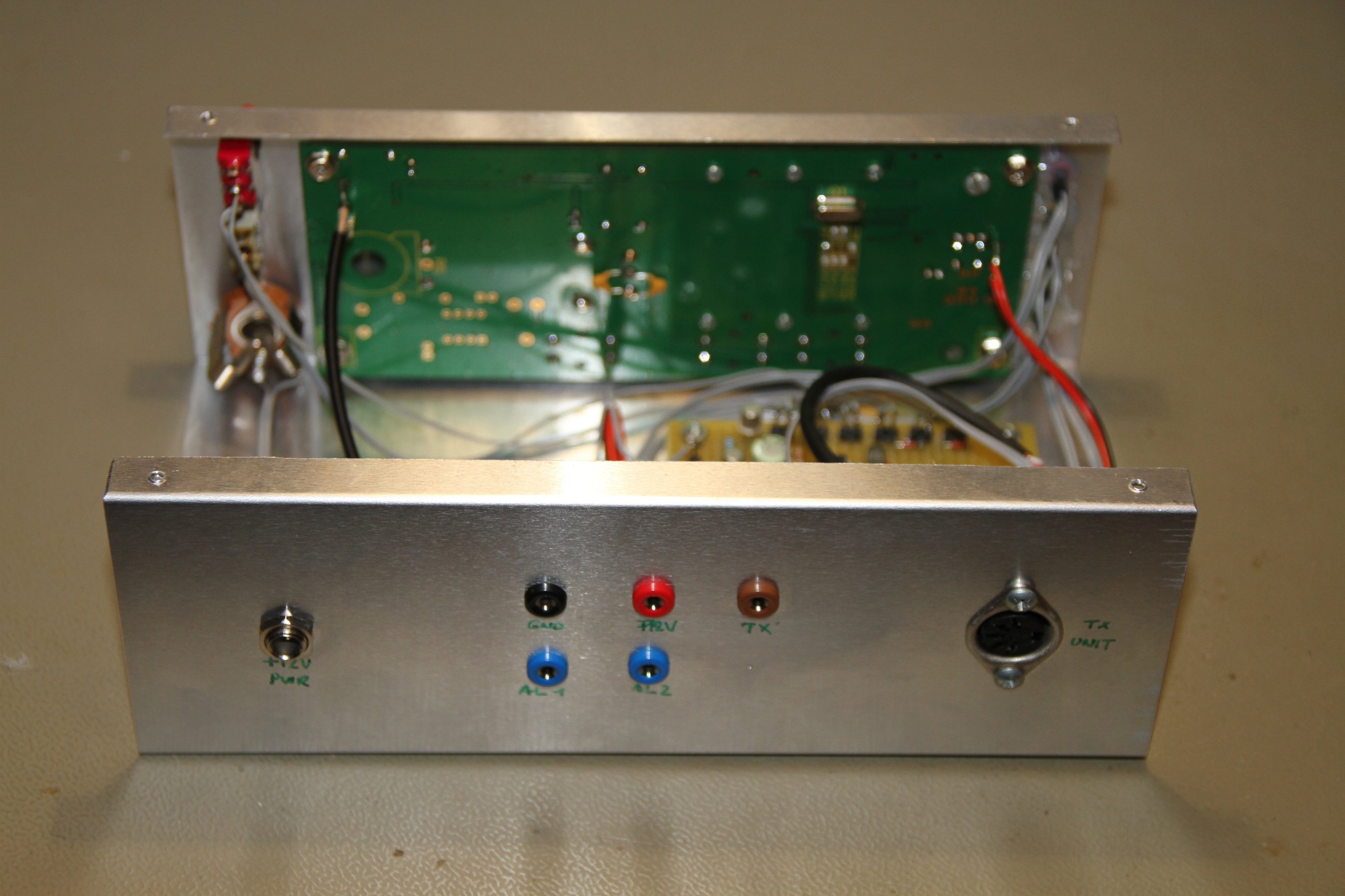
Driver unit, back view (click to enlarge).
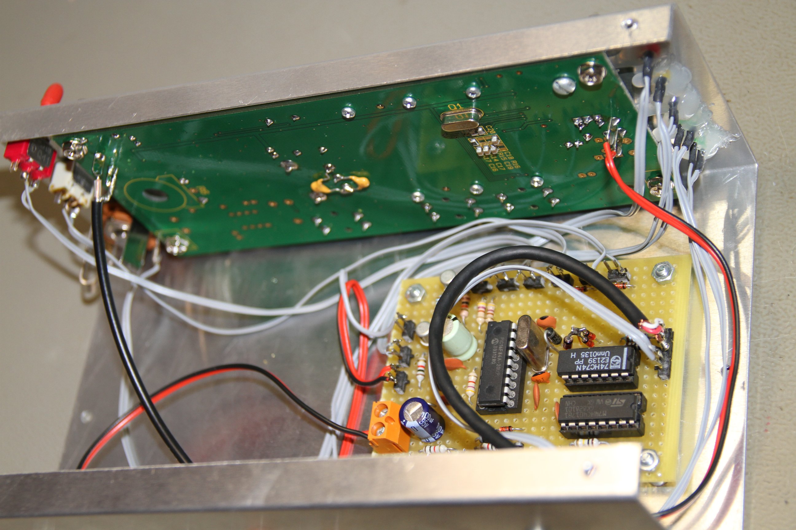
Driver unit, left view (click to enlarge).
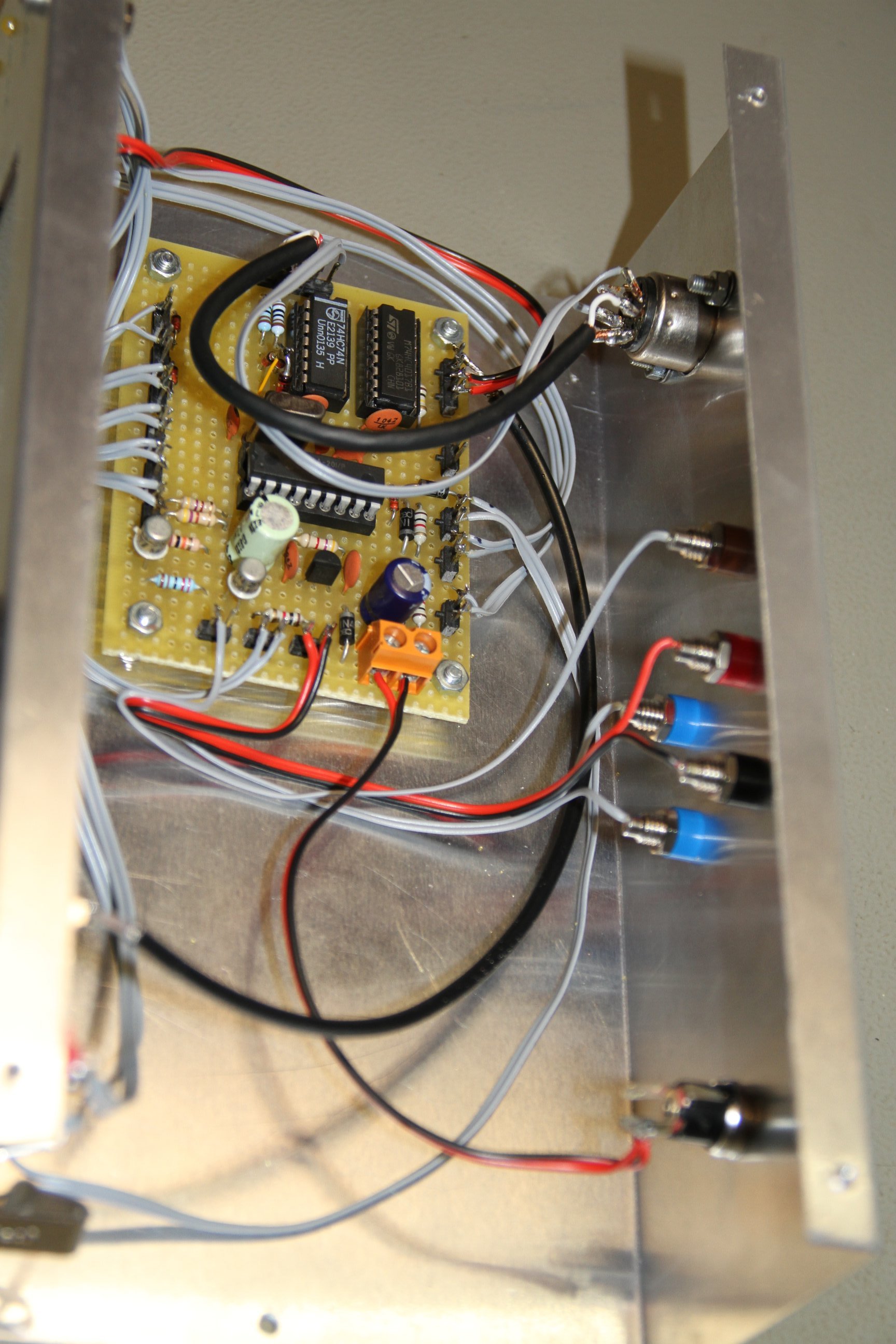
Driver unit, right view (click to enlarge).
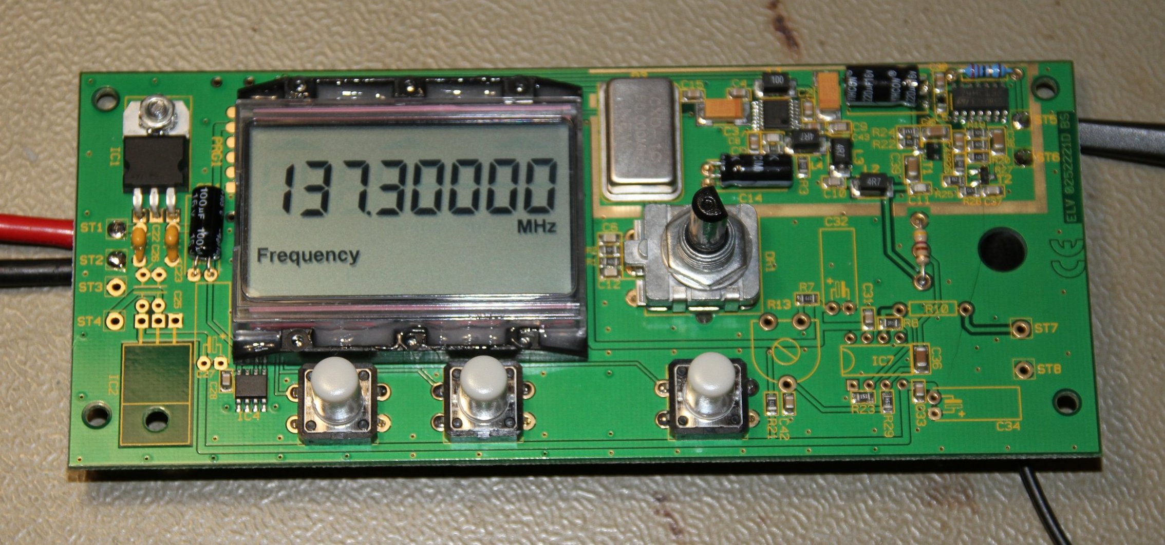
DDS module (click to enlarge). Remark the "MHz" sign meaning "kHz".
| Home | Electronics | Index | Previous page | Next page |