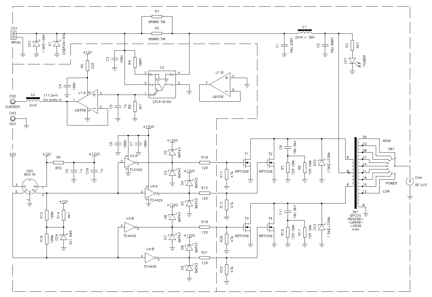
Circuit diagram of the final unit (click to enlarge). – A PDF version is also available: finalcircuit.pdf (47,086 bytes).
The final unit is the power amplifier of the whole transmitter. It's by far the trickiest and bad tempered unit of the whole project; when something is wrong one or more MOSFETs usually blow up some times also destroying other components nearby and one has to be very patient and keep perseverating to get it to work properly.
The carrier is generated and modulated in the driver unit and enters this unit on CN5; it's composed by two complementary TTL signals. The same connector also carries the power supply for the control circuits; both 5 V and 12 V rails are connected but only the 12 V is used.
MOSFET gates are driven through TC4426 driver ICs. These drivers are inverting, meaning that the lines on CN5 must stay high when the transmitter is idle. To make sure the MOSFETs will not conduct when manipulating the connector (or in case of a false connection) R15 and R19 pulls these lines to 5.1 V. The 5 V line on the connector is not used and an auxiliary 5.1 V is generated by R14 and DZ4 from the 12 V line; this is because when the connector is manipulated, it's not possible to know which line will connect or disconnect first, so the pull-up resistors must use the same power supply as the gate driver ICs.
Two TC4426 have been used because the gate capacitance of the power MOSFETs used here (IRFP250) is pretty high (about 2 nF) and just one IC wouldn't supply enough current to be effective at 500 kHz. Diodes D2 through D9 protect the ICs when the MOSFETs blow up and resistors R10, R12, R18 and R21 limit somehow the switching time to prevent the voltage on the drains from overshooting too much. Resistors R11, R13, R20 and R22 make sure the MOSFETs stay off if a TC4426 blows up.
R9, C9 and C10 are used to filter the power supply: the two capacitors are a local energy storage used to charge and discharge quickly the gate capacitance of the MOSFETs and the resistor prevent high current spikes from flowing in the power supply line. The capacitors must be mounted very close to the driver ICs.
Circuit diagram of the final unit (click to enlarge). –
A PDF version is also available: finalcircuit.pdf (47,086 bytes).
This amplifier uses a push-pull transformer configuration. After having made it to work, this is probably not the best choice as energy in the transformer stray inductance causes voltage overshoots: it cannot be recovered to be sent back to the supply rail and requires lossy snubber networks. A better choice would be a single ended totem-pole configuration, but this requires a completely different gate driver circuit; so it has been decided to leave the final unit as is, but the configuration should be reconsidered in case of a new design.
Transformer T1 is the heart of the amplifier. It's built on a large toroidal core made of N30 ferrite material. This material has a μ of 4300 and an AL of 5.4 μH: only a few turns make a large inductance. The secondary winding is composed by 36 turns of 1.2 mm-diameter enameled copper wire with several taps. By selecting a tap with SW1 the output power can be adjusted; more turns correspond to a higher power. For exemple, with a power supply of 40 V, a power of 520 W is obtained with 36 turns and the power is reduced to 85 W with only 12 turns. Do not operate SW1 while transmitting!
The primary winding is composed by 8 turns of bifilar PVC-insulated 1 mm2 cross-section electric cable, coiled over the secondary. The number of turns is selected from the power supply voltage: 8 turns are fine with 40 to 50 V, lower voltages may require less turns, but than there is a risk of core saturation. Higher voltages should be avoided because the maximum VDS voltage of the MOSFET may be exceeded.
MOSFETs are paralleled two by two to reduce the on resistance of their channel. The center tap of the primary winding is connected to the (filtered) supply voltage and the MOSFETs short to ground each side of the primary in a symmetrical manner. When one MOSFET is open, it sees twice the supply voltage on it drain because of the induced voltage in the other half-primary. IRFP250s can handle drain voltages up to 250V.
Because of the stray inductance of the transformer, each time a MOSFET opens an overshoot voltage is generated and this will end in a dangerous ringing waveform, as shown in the picture below:
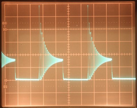
MOSFET drain voltage, no snubber network, 8 V supply voltage, 10 V/div, 2 μs/div.
This is what happens when the snubber networks C8-R7-R8 and C11-R16-R17 are not there. To prevent damages to the MOSFETs, a supply voltage of only 8 V instead of 40 V was used. One can now measure the frequency of the ringing (3.58 MHz in this case) caused by the stray inductance (mainly in the transformer) and the stray capacitance (mainly in the MOSFETs). By temporarily paralleling a capacitor (say 10 nF or so) across drain and source the frequency of the ringing lowers (here to 1.7 MHz) and with some algebra and the famous formula f = 1 / ( 2π √ L C ) it's possible to determine the stray inductance and stray capacitance: here we have 0.56 μH and 3 nF. Now we can design the RC snubbers: the capacitance of the snubber must be larger than the stray capacitance we just calculated and a value of 10 nF was selected. The resistor should match the impedance R = √ L / C , about 12 Ω. As one can see in the figure below, adding the snubbers completely kill the ringing and the overshoot is much less:
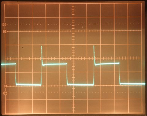
MOSFET drain voltage, 15 Ω — 10 nF snubber network, 8 V supply voltage, 10 V/div, 2 μs/div.
Than, by doing some testing while increasing the power supply voltage, the resistor value that minimizes the overshoot was found to be around 7 Ω: two resistors of 15 Ω in parallel do the job nicely. If you build this final unit, you'll probably have to retune the snubbers, since stray inductances an capacitances will probably not be the same.
This amplifier provides a square wave, but because of the low-pass filter connected on its output, here we can see that the waveform is a bit wavy. The overshoot is about 140 V and we are on the safe side.
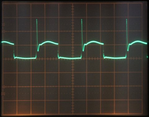
MOSFET drain voltage, 7.5 Ω — 10 nF snubber network, 40 V supply voltage, 50 V/div, 2 μs/div.
To protect the MOSFETs, two surge arrestor diodes DZ2 and DZ3 take care of any voltage spike over 220 V. These diodes only work on sporadic surges; they wont last long if the overshoot is not damped correctly by the snubber networks.
The positive supply line of the amplifier must be filtered to prevent RF from leaking and causing RFI. This is done by the PI filter composed by C1, L1 and C2. L1 is not easy to find: it must be a large inductor (say 1 mH or more) and must carry the full DC current (say 30 A) without saturating! Any closed ferrite core inductor (toroidal, double E, pot,...) will already saturate with a much lower current and a huge air-gap is mandatory. The wire used must also be large enough to carry the current without introducing a too high stray resistance. I finally found a suitable inductor in a loudspeaker crossover filter: a 1 mH air-core inductor made with 1.5 mm diameter enameled copper wire having a DC resistance less than 0.1 Ω. By adding a small ferrite rod in the middle I could increase the inductance to 2 mH.
Since inductors don't like changing currents, protection diodes D1 and DZ1 avoid large voltage overshoots when manipulating the CW key or when the cables are disconnected. In this whole unit, the largest voltage is under 250 V, therefore 250 V capacitors are enough; I used higher voltage ratings just because I had those capacitors on hand.
The two 5 mΩ precision resistors R1 and R2 are used to sense the supply current. U2, a "high side current sense" type LTC6101HV, amplifies the voltage drop of R1-R2 and converts it to a current flowing to ground. This is converted back to ground reference voltage by R6. R4 and R6 sets the gain of this stage and, with the selected values, each Ampere of main current will produce 117.5 mV across R6. C5 filters any RF residue that could be still present, U1:A is just a unity-gain voltage buffer to avoid any load impedance error; U1:B is not used. R5 and C4 are there to filter the power supply of U1 and L2 prevents any noise picked up by the connection wire to leak inside.
Use large cross-section wires for the power supply line, at least 6 mm2, and keep them as shot as possible.
The efficiency of the amplifier is pretty high, over 90%. The four MOSFETs are mounted on two large heat-sinks and the box cover is a perforated metal sheet allowing sufficient ventilation. This is enough for CW operation, but for QRSS operation where the transmitter is operating at full power for long periods of time, a small fan my help keep the unit cool.
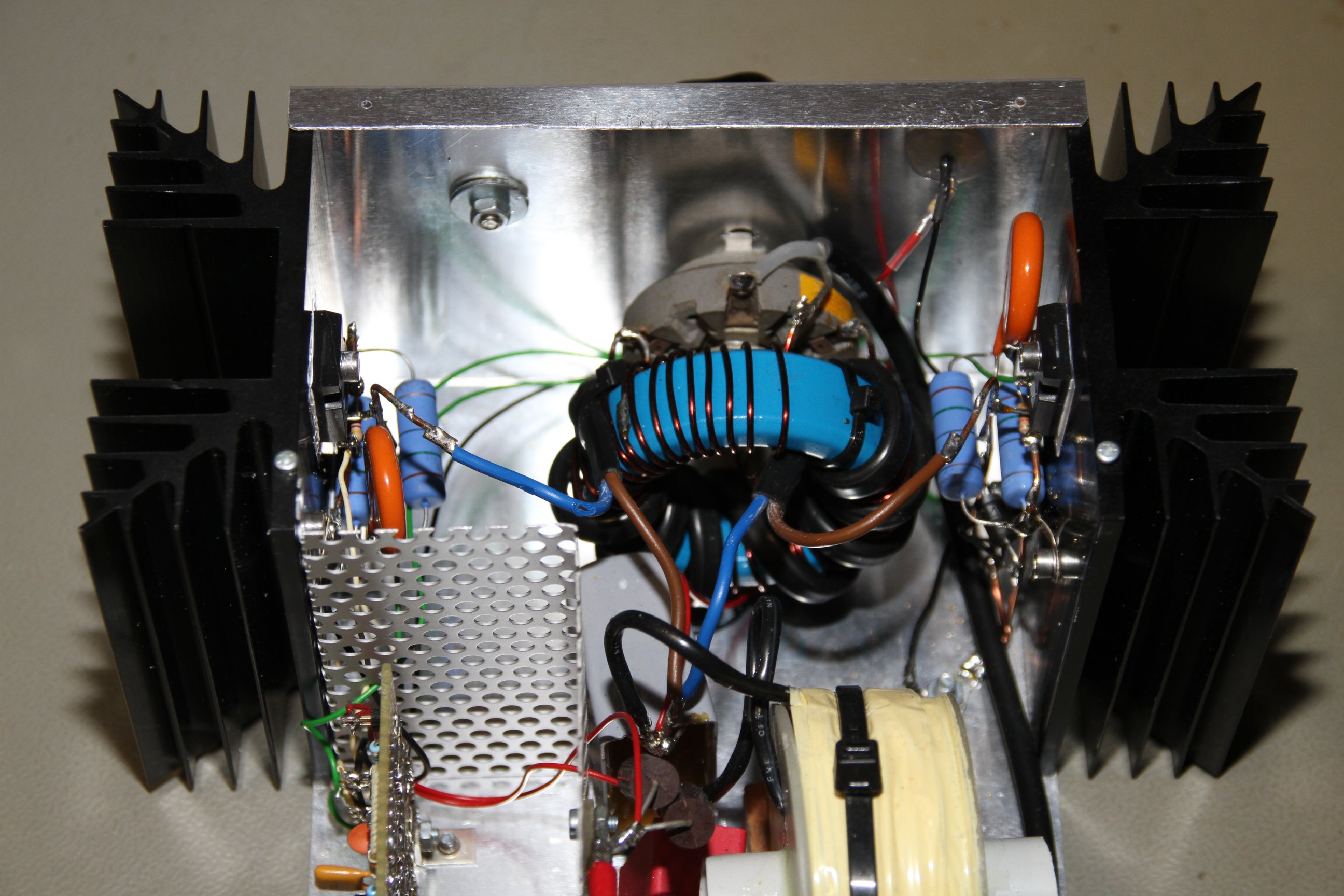
The pictures below show the assembled unit. Please remark the large yellow filter inductor L1 and the blue output transformer TR1 just behind the power selector switch SW1.
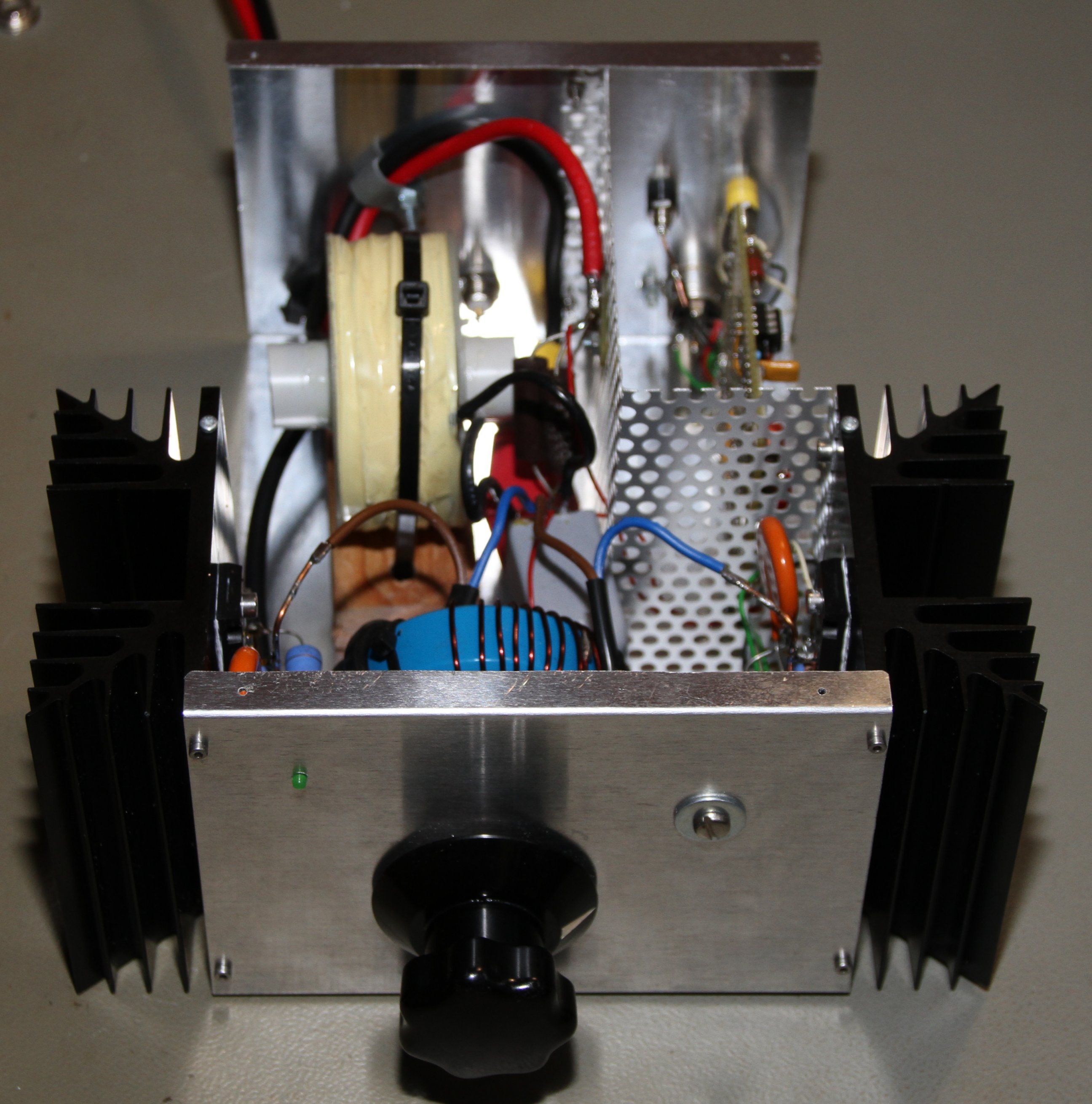
Final unit, front view (click to enlarge).
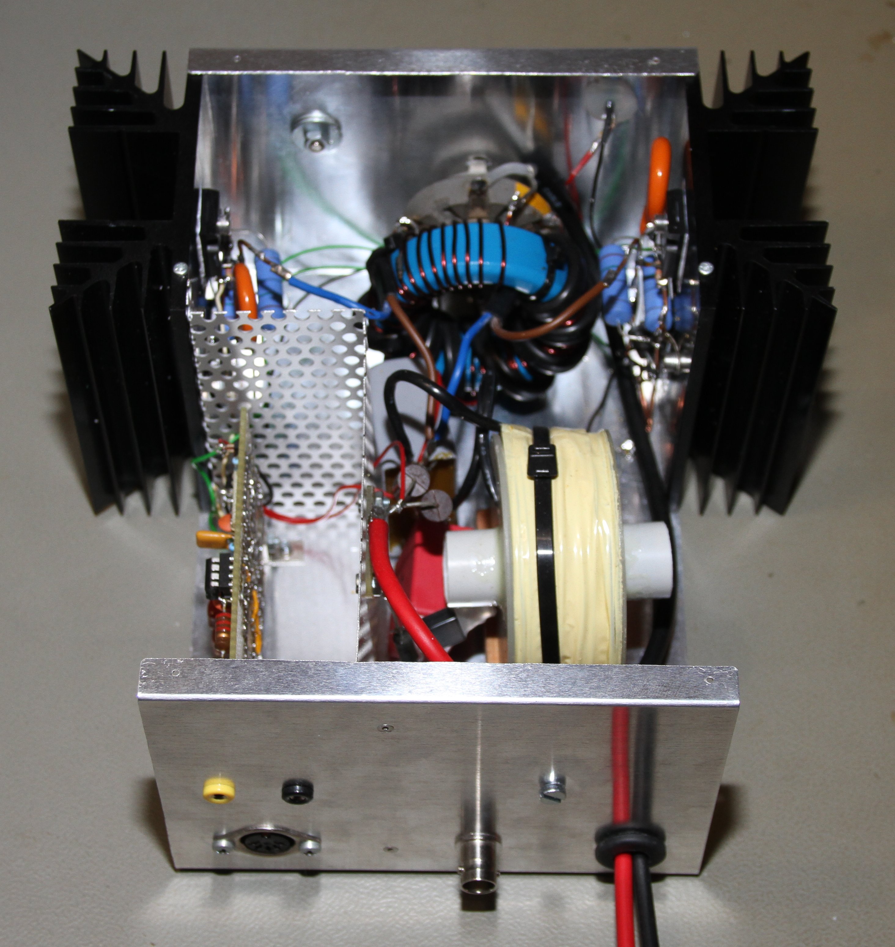
Final unit, rear view (click to enlarge).
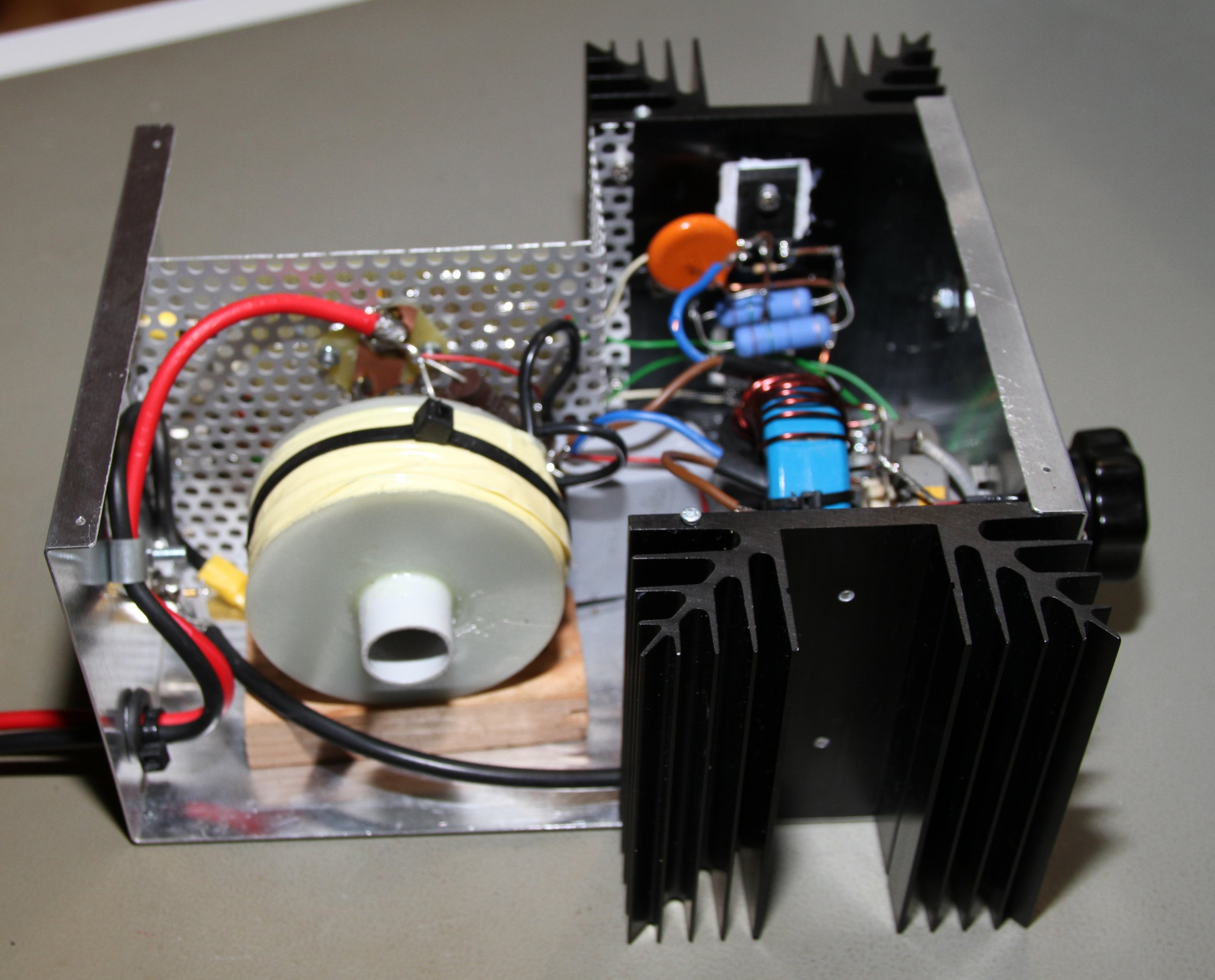
Final unit, side view (click to enlarge).
Final unit, power transformer (click to enlarge).
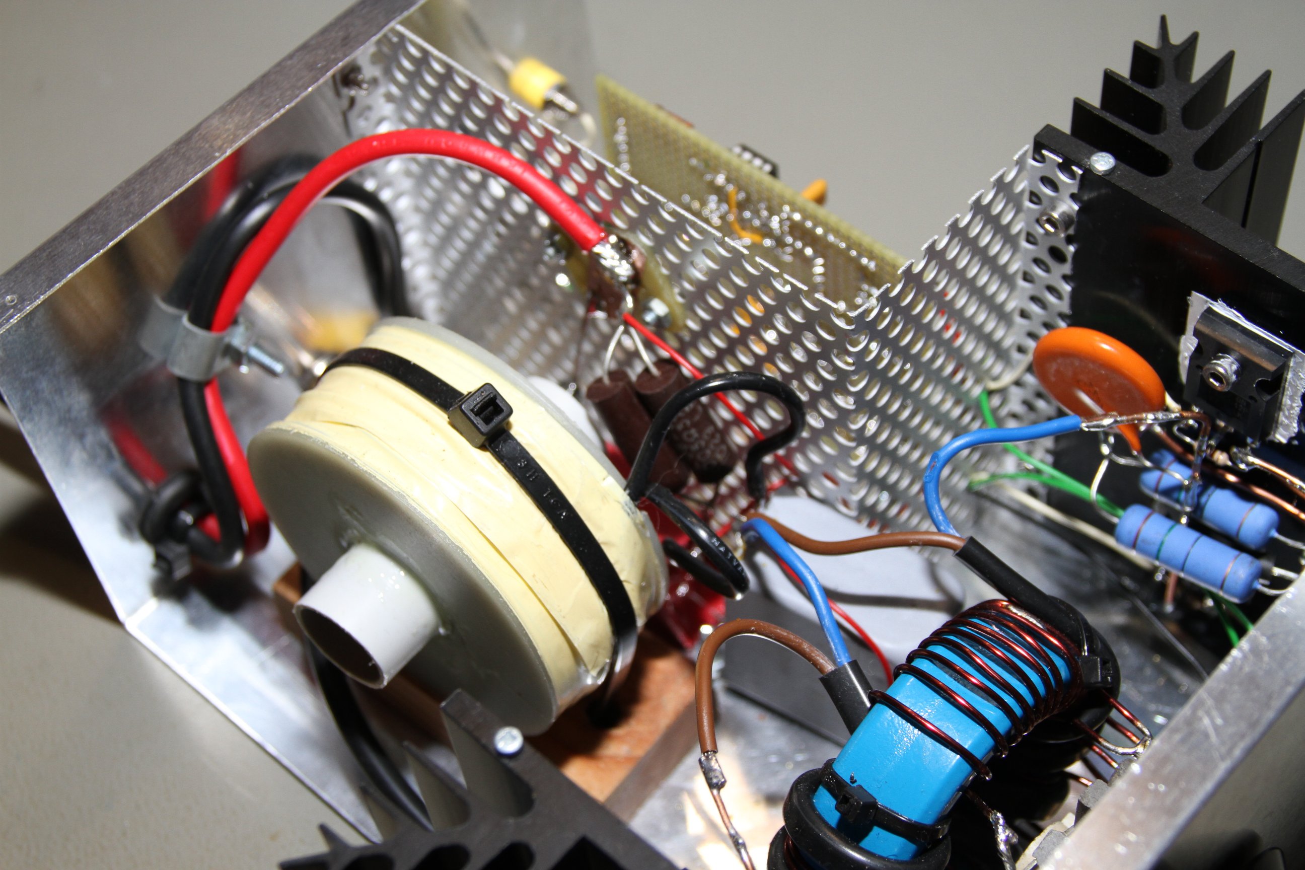
Final unit, DC filter (click to enlarge).
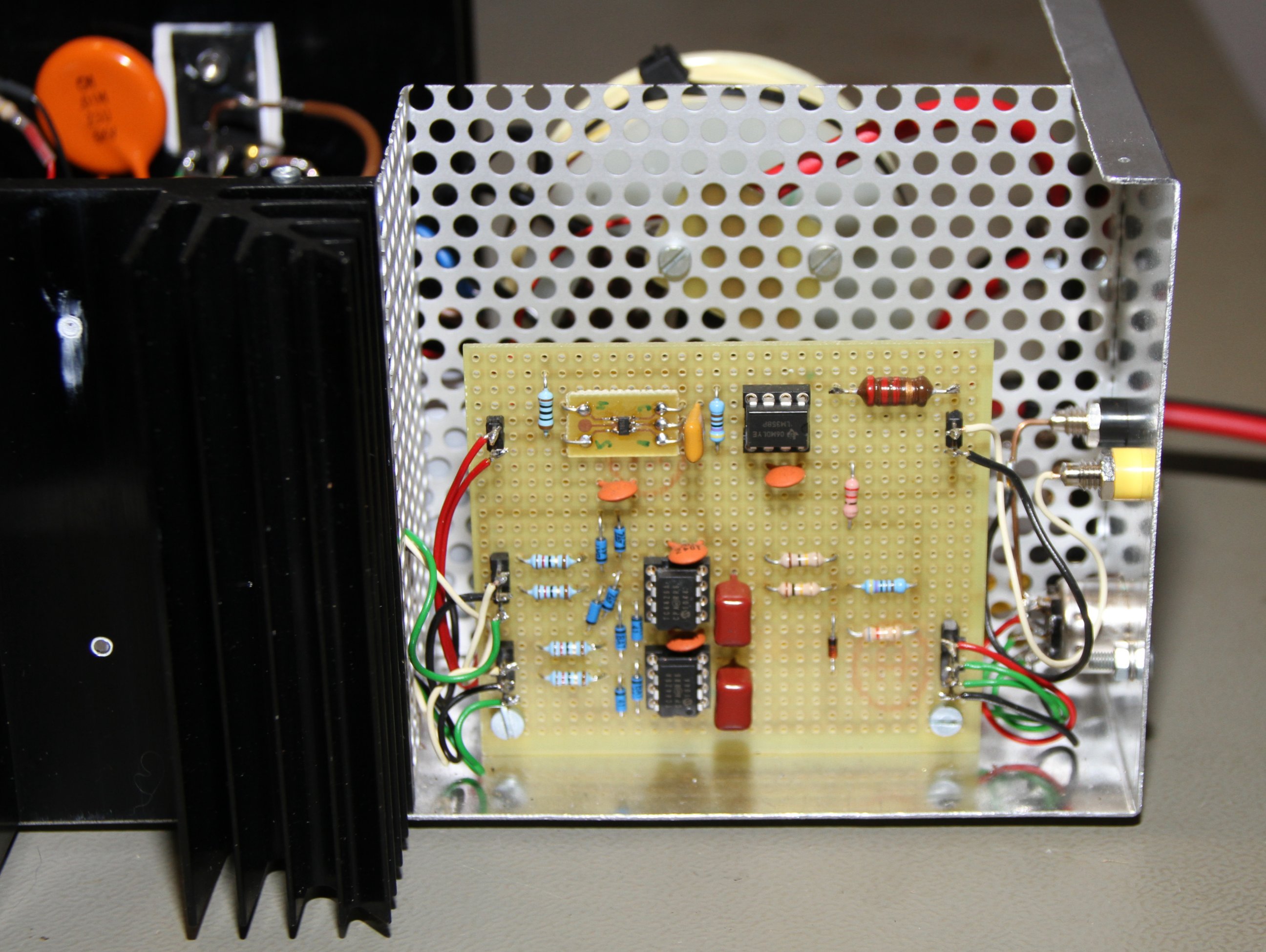
Final unit, MOSFET driver and current sense circuits (click to enlarge).
| Home | Electronics | Index | Previous page | Next page |