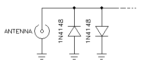
Typical antenna input circuit with protection diodes.
I always had the habit of protecting the antenna input of many receiver circuits with a couple of back to back silicon diodes as visible in the picture below. This protects (within reason) a delicate circuit from unwanted strong signals applied to its input, such as switching on a nearby transmitter and having too much RF coupled to it or shorting to ground any static charge that may accumulate on an well insulated antenna. But I never spent time in investigating the additional distortion this circuit introduces, and this is the goal of this page.
Typical antenna input circuit with protection diodes.
The basic idea of the diode clipper is that for signals with an amplitude within ±0.7 Vpeak (less than about +7 dBm over 50 Ω) the diodes are just open circuits and do not interfere; for higher amplitudes, the diodes clip the signal to about ±0.7 Vpeak limiting the maximum power that reaches the receiver at about +10 dBm over 50 Ω, which the vast majority of receiver circuits can easily tolerate. If you wonder why I specified +7 dBm for unclipped signals and +10 dBm for clipped ones of the same peak to peak amplitude, it's because unclipped signals are supposed to have a nice sinusoidal shape; once clipped, they become more square and their RMS voltage is higher, explaining the 3 dB difference.
Now, this very simple diode model, where a diode is an open circuit for voltages below 0.7 V and clips at 0.7 V any higher level signal is just enough to estimate the limiting power, but is too simple to calculate the distortion on small (unclipped) signals. Diodes are non-linear devices often used in mixers and frequency multipliers, so they must introduce distortion. Now the question is: how much distortion? And is it acceptable?
Now, the circuit that we want to simulate is basically a voltage divider with two diodes back to back as shown below:
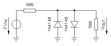
The circuit to simulate, the voltage source with its internal
resistance is on the left, the two clipping diodes in the middle and the load
is on the right.
The internal resistance of the generator (left) and the load resistance (right) are the two resistors of the divider. All impedances are supposed to be matched (both resistors are equal). The standard impedance of 50 Ω was selected because is the most common value for radio frequency circuits.
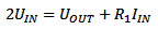
Very often, these two resistors are not "real" resistors, they are just how the source and load impedance look like, but they form indeed a voltage divider and the load voltage is half of the source voltage (when diodes don't clip). In practice, we don't have access to the true voltage source, and this 1:2 ratio is annoying. To avoid it, the source voltage is specified as 2·UIN, so that UIN is the voltage that appears on the load (UOUT) when no diodes are connected and we can compare what happens with and without the diodes without bothering with the 1:2 ratio.
The first attempt to simulate this circuit was done with a free SPICE simulator software, but rounding errors were too high for calculating any harmonic distortion or third order intercept point: it generated a strange and unrealistic noise floor 60 dB below the main signal. So a different way of simulation had to be found.
Finally, since the circuit is quite simple, I decided to directly calculate the output voltage in the old "pencil and paper" way. But for this, a good diode model is required.
The Shockley ideal diode equation is used here because it allows calculating precisely what happens for small and large signals. It relates the diode (forward) current ID as a function of diode (forward) voltage U.
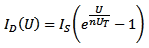
It's an exponential function and depends on U, but also on three parameters that we consider constant for this simulation. The reverse bias saturation current IS and the emission coefficient n depend on the particular diode we want to simulate. Here, to simulate the famous 1N4148, we chose IS = 4.352 nA and n = 1.906 (these values are the ones specified by NXP in their SPICE model). Here we used a thermal voltage UT = 26 mV corresponding to a (room) temperature of 300 K and taken as constant. Small thermal variations are out of scope for this discussion.
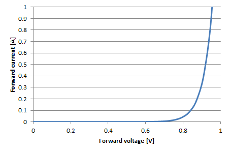
Diode forward current as a function of diode forward voltage of a 1N4148 according to the Shockley equation.
If we plot this equation, we get the above curve: it corresponds well to what we expect from a general purpose silicon diode such as the 1N4148.
The circuit to calculate can is completely described by the following two equations that are just the application of Kirchhoff laws:
 ;
;
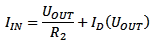
ID(UOUT) is, of course, the Shockley equation described before. By combining and rearranging these two equations, we obtain the following:
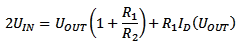
Now, the above equation gives UIN(UOUT) while we are looking for UOUT(UIN). But solving for UOUT cannot be done analytically because of the exponential in the Shockley equation (or, if it can, I couldn't do it). So, I ended up in solving it numerically, using MS Excel, its numerical solver and some macros; it's not very elegant and is terribly slow, but finds a solution with the required accuracy and was readily available.
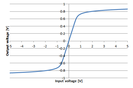
Transfer function of the diode clipper.
The calculated transfer function is visible in the above plot. As expected, it's about linear between ±0.6 V, for higher amplitudes se signal is compressed around ±0.7-0.8 V. This is a smooth curve and has no sharp angles.
Please remark that in this simulation, only the forward polarized diode is taken into account. The other diode is supposed to conduct no current: this greatly simplifies the calculation.
Now that we have a nice model for the diode clipper, we can feed it with some sinusoidal input signal to calculate with good accuracy the clamped signal at the output. Then, with an FFT, we can precisely analyze the harmonic content of the output signal. By repeating this process for different amplitudes, it is possible to have an idea of the maximum signal that will go through the clipper undistorted (or with an acceptable distortion).
Several amplitudes have been used for this simulation: –100 dBm, –80 dBm, –60 dBm, –50 dBm, –40 dBm, –30 dBm, –20 dBm, –10 dBm, –5 dBm, 0 dBm, +5 dBm, +10 dBm, +15 dBm, +20 dBm, +25 dBm and +30 dBm. The typical signals that can be found on a receiver antenna connector range from –140 dBm to –30 dBm, –73 dBm being the standard S9 signal, already considered strong. There is no need to simulate signals weaker than –100 dBm because already at –100 dBm distortion is so low that cannot be calculated. On the other hand, signals up to +30 dBm have been simulated to see what happens when the clipper really does its job.
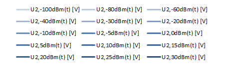
Legend for the signals plotted in the following two figures.
In the figure below, all input signals are displayed. With a linear scale, only the strongest ones are clearly visible.
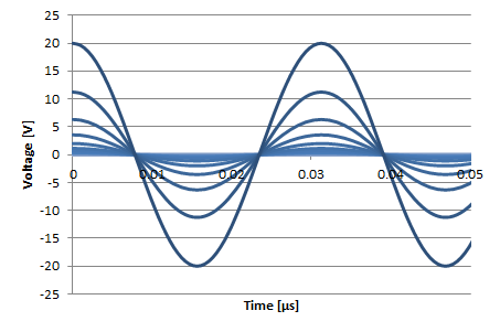
Input signals ranging from –100 dBm to +30 dBm.
The figure below shows how the signals look like after the clipper. Again plotted on a linear scale, the compression is clearly visible: the strongest signals (that exceeded several Volts before the clipper) are now within ±1 V and have a "square wave" appearance, while the weak signals go through undistorted and keep their sinusoidal shape.
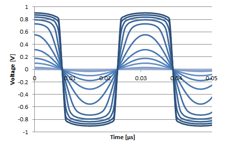
The same signals as in the previous image after clipping.
To perform reliable FFT on this numerical model, a few tricks are necessary: first, the FFT algorithm works only with a sampling period containing a number of samples which is an integer power or 2; here we used 1024 samples (= 210). Than the signal to analyze must have an integer number of cycles in the sampling period, otherwise spurious signals will appear, polluting the result. Since the model is not frequency dependent, we arbitrarily chosen a sampling frequency of 1024 MHz, a sampling period of 1 μs (1024 samples, one every 0.977 ns), and a test signal of 32 MHz. With these conditions, it has exactly 32 full cycles in the 1024 samples. This gives an FFT resolution of 1 MHz, which is also handy.
Again, the simulation is calculated with MS Excel, its built in FFT function and some macros. As before, not elegant and slow but provides accurate results.
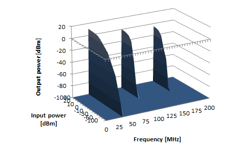
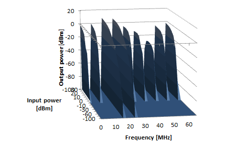
Waterfall plot of the FFT analysis of the diode clipper using a 32 MHz signal.
The result of the FFT is displayed in the above 3D plot. As one can see, for input signals below 0 dBm, the harmonic content is very low, but for stronger signals distortion rapidly appears with stronger and stronger harmonics.
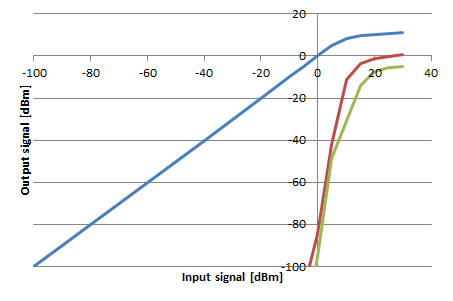
Frequency domain transfer function of the diode clipper.
Blue: fundamental frequency,
red: third harmonic,
green: fifth harmonic.
Another way to look at it is in the frequency domain transfer function displayed above. We note that for low amplitudes, say below a few dBm, the clipper is linear and has a slope of 1 (the same signal goes through undisturbed). Distortion (harmonics) is almost non-existent in this region. At about 0 dBm third and fifth harmonics start to appear and grow very rapidly. At the same time, the transfer function shows a knee and even for strong input signals, the output does not exceed +10 dBm, as expected from a clipper.
Third order intercept point (IP3) is closely related (and very similar) to harmonic distortion. To evaluate its value the same analysis as before has been repeated using a superposition of two signals at two different frequencies, but with the same amplitude. The result has been analyzed in the same way. Since both signals must have an integer number of cycles in the 1024 samples, the frequencies of 16 and 24 MHz have been arbitrarily selected. They have respectively 16 and 24 cycles. Since the model is frequency independent, there is no reason to use frequencies very close to each other as one would use in a real life test.
Waterfall plot of the FFT analysis of the diode clipper using two
signals at 16 and 24 MHz.
The 3D waterfall graph (above) is now more crowded but very similar as before. One can easily see both input signals at 16 and 24 MHz and the third order intermodulation products appearing at 8 and 32 MHz for input signals stronger than about 0 dBm. Other higher order intermodulation products are visible as well.
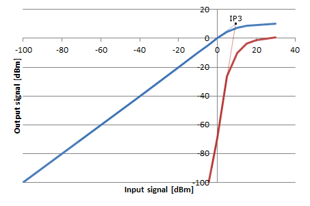
Frequency domain transfer function of the diode clipper.
Blue: fundamental frequency,
red: third order intermodulation products.
On the above frequency domain transfer function, the third order intercept point (IP3) is clearly visible and is at +10 dBm. Since the slope of the transfer function is 1 (same amplitude for input and output signals), there is no difference between input and output third order intercept points (IIP3 and OIP3 respectively): they both are +10 dBm.
In order to verify what has been calculated before, some real measurements are a must. Here, a 1 MHz sinusoidal signal was used. Real life is not frequency independent and a "low" frequency such as 1 MHz allows neglecting the length of diode leads and the stray capacitance introduced by the diodes themselves. The two diodes are, of course, a pair of 1N4148. The result is shown in the waterfall plot below:
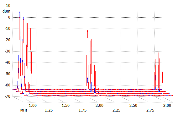
Measured spectra of a 1 MHz signal at four different amplitudes:
+4 dBm, +1 dBm, –2 dBm and –5 dBm.
Blue: no diodes, just the input signal.
Red: diodes connected.
As one can see, for amplitudes below –5 dBm, no harmonics can be observed, but as the amplitude rises, as expected, harmonics appear and grow rapidly. This corresponds to the expectations.
But there are differences with the previous theoretical model: one is that in practice the input signal is not perfectly a pure sine wave and has already some harmonic content (blue traces). As expected, these harmonics are increased by the clipping action of the circuit.
Another difference is a strong presence of even harmonics, while in our theoretical model, only odd harmonics appear. I suspect that is due the two diodes not being identical and not clipping the signal symmetrically, but I didn't investigate this any further.
One important question is: what is the maximum power that we can feed to the clipper without damaging it? According to the NXP datasheet, a 1N4148 diode can withstand a continuous DC current of 200 mA and can dissipate maximum of 500 mW. Let's first calculate what is the power dissipated by the diode at its maximum current: 200 mA · 0.7 V = 140 mW. Since this is lower than its maximum power rating of 500 mW, we will use 200 mA in our calculation, otherwise we would have to use a lower current. When the diodes are clipping, the load impedance is no longer 50 Ω because of the diodes somehow shorting it to ground. Since current in the diodes is much larger than the current in the load, we will neglect the latter and consider that all current is flowing through the diodes. When a power source delivers half of the diode maximum current on a 50 Ω load, here 100 mA, it delivers (100 mA)2 · 50 Ω = 0.5 W of power. When the same source is connected to our clipper it will no longer be matched to 50 Ω because of the diodes appearing like a short circuit: the current will tend to double (our maximum 200 mA) and the power will drop significantly because voltage is now limited around 0.7 V. Therefore we can say that the maximum safe power source than we can connect is around 0.5 W (27 dBm).
Higher ratings diodes will certainly resist a higher power, but will probably have the disadvantage of introducing more stray capacitance. Each 1N4148 will add 4 pF: depending on the frequency this may or may not be a problem, and may require compensation. For example, if there is a low-pass filter after the clipper, is easy to compensate for the extra stray capacitance, just by reducing the parallel input capacitor.
Diodes often (but not always) show a nice feature: when too much power is applied, they will of course blow up; but after blowing up, they become a short circuit. In this case, even if the diodes are dead, they are still protecting the rest of the circuit. So, even if an overload does occur, there are still good chances that only two diodes of the clipper are faulty.
Not every diode is suitable for this circuit: fast diodes are needed. 1N4148 have a switching time of 4 ns and are good up to a few dozen MHz; for higher frequencies, faster diodes should be used.
The effect of two back to back diodes in parallel with a receiver antenna connector has been analyzed. Their effect is negligible for weak signals, say below –20 dBm, it becomes observable around 0 dBm and the clipping action limits the maximum power around +10 dBm. The IP3 has been calculated to be +10 dBm.
If this is acceptable or not depends on the application. A diode clipper will certainly ruin the performance of a professional top of the line +30 dBm or more IP3 receiver, but can accepted in many other cases: when the receiver is just good but not a top performer, or when the antenna is located and designed in such a way that it doesn't pick up strong signals, or when a narrowband filter prevents strong signals to reach the clipper.
| [1] | Dr. F. Rahali, Prof. M. Declercq. Électronique I, partie 2: dispositifs à semiconducteurs. École Polytechnique Fédérale de Lausanne, 1996, chapitre 8. |
| Home | Electronics | Page hits: 022220 | Created: 09.2014 | Last update: 09.2014 |