In the last years medium-wave (MW) amplitude-modulated (AM) broadcast stations are gently disappearing, at least in Europe. For people who like vintage radios (wooden radios!) this is a bad news: because of the specific propagation characteristics of this band only the local station can be received during the day, since ionosphere propagation is completely blocked by the D layer. If the local station has been switched off as it was the case end of 2010 with the Sottens transmitter that was the last Swiss MW transmitter, one has to wait the evening when the D-layer disappears and medium waves can be reflected by the E-layer to hear some stations on this band.
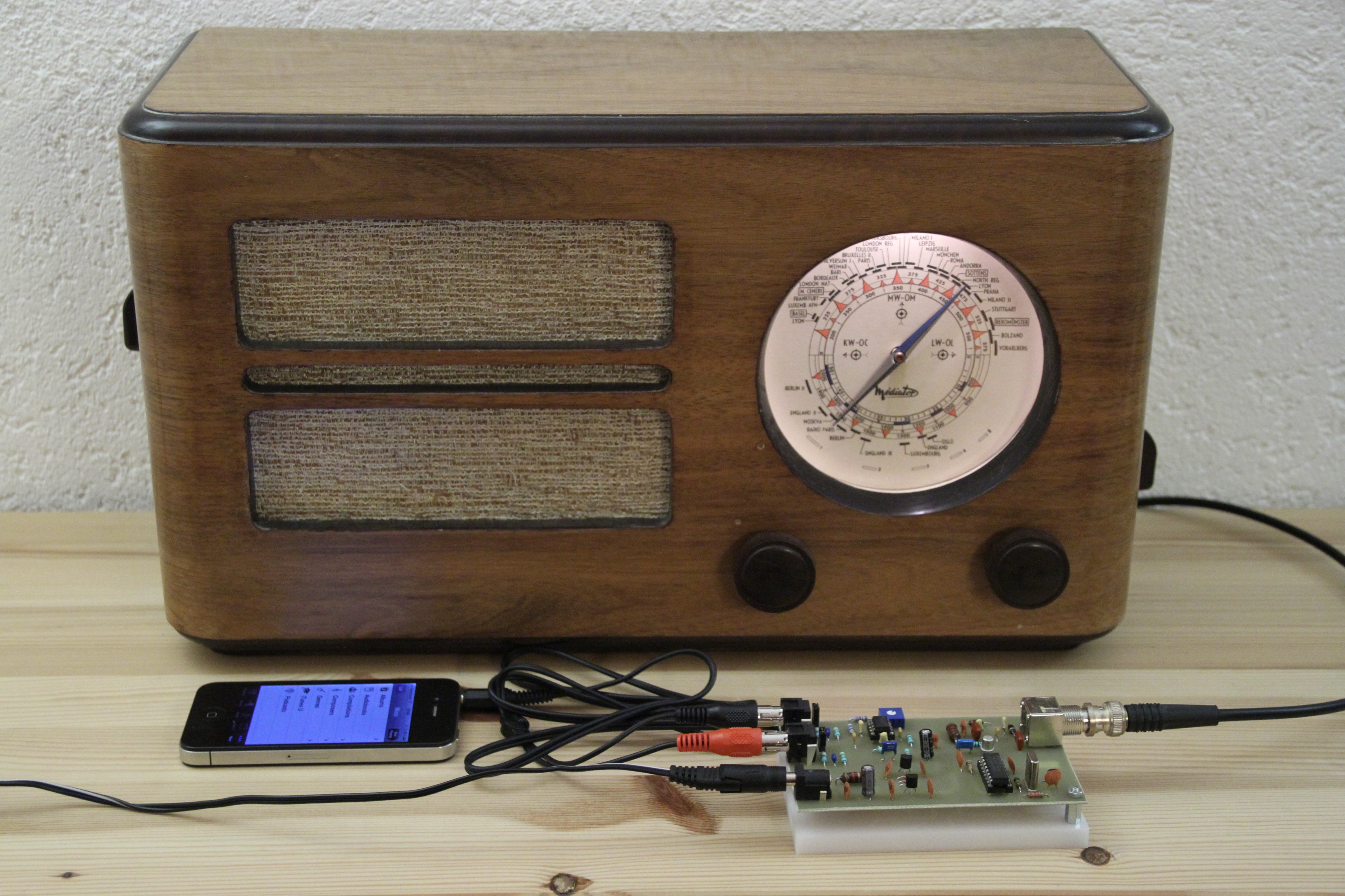
It's easy to buy an MP3 player FM modulator for a cheap price, but bad luck: vintage radios do not have (or very rarely) the FM VHF band. So the idea described in this page is an AM modulator for the MW band that will allow hearing the music of a CD or MP3 player during daytime on such radios. This is not a transmitter: the output power is very low (only 10 mW) and is intended to be connected to the antenna input of the radio, or to be closely coupled with it. Amplifying the signal would be a bad idea, since transmitting in this band is strictly forbidden in many countries.
The complete circuit is visible in the figure below. Click for a larger version with all details.
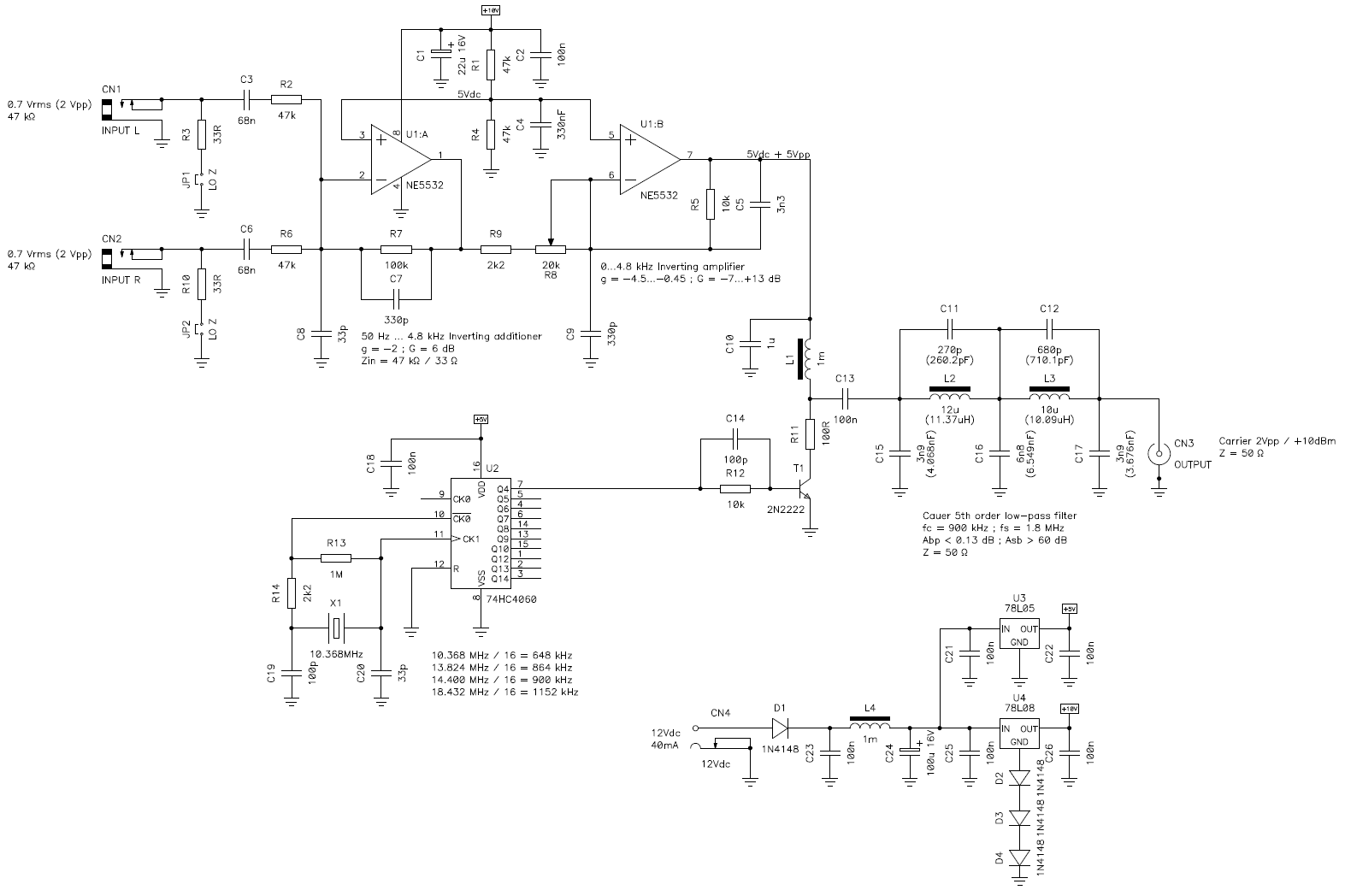
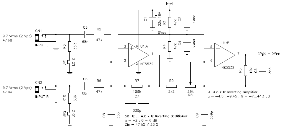
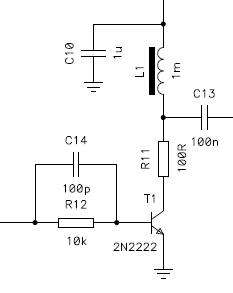
The audio signal is connected to CN1 and CN2. The input stage is designed for stereo signals of 0.7 Vrms (2 Vpp) and has an impedance of 47 kΩ because this is usually what is needed to connect the line output of a CD player. If one wants to use the earphone output of an MP3 player, shorting JP1 and JP2 will drop the input impedance to 33 Ω to match this kind of output. AM only supports mono signals, so both channels are just added together in U1:A. In case of connection of a mono signal source, one can use either CN1 or CN2, but should always short the jumper of the other channel to make sure it doesn't pick up noise.
The RC networks C3-R2 and C6-R6 limit the lower side of the bandwidth to about 50 Hz preventing DC from shifting the bias of the modulator. U1 is an ordinary NE5532 low noise audio operational amplifier. U1:A is just an inverting additioner with a gain of -2 (6 dB). The network R7-C7 limits the upper part of the bandwidth to about 4.8 kHz. U1:B is an inverting amplifier whose gain can be adjusted via R8 between -0.45 (-7 dB) and -4.5 (+13 dB). This is used to adjust the modulation factor as close as possible to 100 % according to the exact amplitude of the input signal. To avoid distortion, 80 % will be good enough, since power efficiency is not an issue for this application. If this range is not enough, one could change R9 and R8 to increase or decrease the gain. The network R5-C5 limits again the upper edge of the bandwidth of this amplifier to 4.8 kHz.
Capacitors C8 and C9 make sure the inverting inputs of the two operational amplifiers are grounded at RF preventing the operating point to shift because of RF leakages from the modulator stage. R1 and R4 bias both operational amplifiers at about 5 Vdc, while bypass capacitors C2 and C4 removes RF leakages from the bias line. Capacitor C1 is used as energy tank to supply the amplifiers during audio peaks. The output of U1:B directly feeds the modulator stage. The bias of this amplifiers directly controls the bias point of the modulator. It was fixed to 5 V to allow voltage swings almost from 0 to 10 V. Changing the bias voltage will reduce the maximum undistorted RF amplitude.
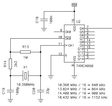
In this circuit, the carrier frequency is generated by a crystal oscillator. Using a VFO was considered for its simplicity, but neutralizing thermal drift will make the circuit more complex to adjust and since old radios do also have significant drift, having a stable frequency would simplify its use and allows using this modulator as test equipment for fixing defective receivers.
In Europe, AM broadcast stations use a 9 kHz channel raster and all carrier frequencies are an integer multiple of 9 kHz. It would be nice if this modulator could match this rule. Ok, one could argue that old radios have a continuous tuning range and can tune in any frequency, but if this modulator is used as a laboratory tool to repair or align more recent receivers, having a correct frequency would be an important feature.
Since it's almost impossible to find a crystal that has directly a suitable frequency in the AM MW band (531 to 1611 kHz in Europe) a crystal with a higher frequency was chosen, requiring the frequency to be divided down. Several standard crystals divided by 16 give correct AM MW carrier frequencies as shows in the following table:
For this project a crystal of 10.368 MHz was used but other crystals will work as well. If the correct channel alignment is not needed, any crystal between 8.496 MHz and 25.776 MHz will work.
The oscillator is a classical 4060 C-MOS oscillator and divider. For this application the 74HC4060 version was used because of its ability to deal with frequency higher than a few MHz and because it produces fast rise and fall time pulses. There is not much to say about this stage: the output frequency, already divided by 16, is available at pin 7 of U2 in the form of 50 % duty-cycle square wave. The other outputs are not used. The crystal oscillator has no frequency adjustment (capacitors C19 and C20 are fixed), since this functionality was considered unnecessary for AM applications.
T1 is used as some sort of D-class amplifier/modulator and works as an ON/OFF switch. The carrier signal at MW frequency coming from U2 drives transistor T1 via R12 and C14. While R12 limits the current in T1's base to reasonable amount, C14 helps T1 in switching fast ON and OFF. Without it, the charge accumulated in T1 base would have to slowly pass through R12 making the switching edges too soft. T1 is just a very common general purpose transistor type 2N2222. Probably, any similar transistor will work fine as well.
The AM modulation is achieved by varying the collector voltage if T1 with the audio signal provided by U1:B and the bias point of the audio amplifier sets the carrier power and peak envelope power available. Since T1 is directly powered by U1:B output, the maximum available current is 30 mA. In order to limit the current used by T1 (and reduce it's power), resistor R11 has been connected in series with T1. In a normal class-D amplifier such a resistor would be a shame, but the goal of this circuit is not to produce high power or high efficiency: we just want a clear modulation at very low power. Reducing or removing R11 to increase the output power would be a bad idea: U1:B cannot supply the extra power and distortion would be dramatically increased.
L1 acts as an RF load for the modulator and also prevents the RF to go back to the audio section. C10 is in charge of shorting to ground any RF signal that leaked though L1. When no audio is present, the modulator is biased at 5 Vdc (imposed by R1 and R4). The audio modulation changes this voltage down to 0 V and up to 10 V during modulation peaks, therefore modulating the output up to 100 %.
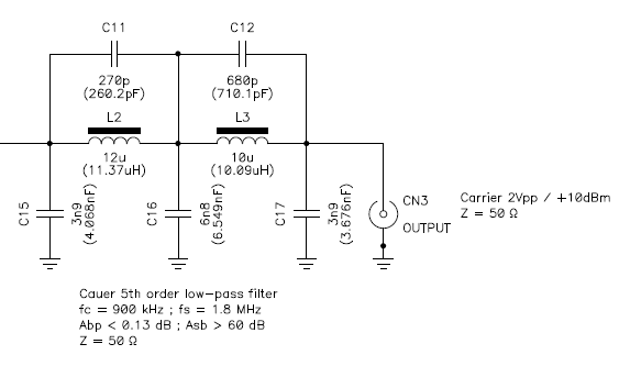
The modulator output goes to the output filters though C13, that preventing the DC present on T1's collector from reaching the output. The output filter is composed by C11, C12, C15, C16, C17, L2 and L3. This is a fifth order Cauer filter with a cutoff frequency of 900 kHz. It's designed to pass all frequencies below 900 kHz with a maximum attenuation of 0.13 dB and block all frequencies above 1.8 MHz more than 60 dB. Nominal impedance is, of course, 50 Ω. Theoretical values are reported in brackets, but of course, only standard values components have been used.
If an output frequency above 900 kHz is used, all filter capacitance and inductance values should be reduced proportionally to shift the cutoff frequency upwards. Halving all values will double the cutoff and stop-band frequencies.
At the output, the carrier level is 2 Vpp on 50 Ω, meaning 10 mW (+10 dBm) of carrier power. The peak envelope power is, of course 4 times higher: 40 mW (+16 dBm).
The whole circuit is powered by an external 12 Vdc power supply such as a wall wart. This has the advantage that no dangerous voltage is present on the board. DC power is applied to CN4 and D1 protects the circuit from polarity inversions. L4, C23 and C21-C25 form a low-pass filter preventing the RF from escaping through the power supply cord. C24 is used as local energy storage and avoid strong current pulses on the supply line.
U3, a 78L05, generates the 5 V supply voltage for the carrier generator that requires a standard TTL power supply like all 74HC C-MOS ICs. U4, a 78L08, generates the 10 V supply voltage for the audio amplifier. Since a 78L08 usually generates 8 V, its output voltage is increases by about 2 V by the three diodes D2, D3 and D4.
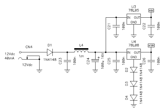
Care should be used in selecting the right power supply for this circuit. All noise introduced by the power supply will be at the modulator output, so cheap switching mode power supplies should be avoided or extra filtering before CN4 will be required. It's also a good idea to install a common mode ferrite choke on the power supply DC cord.
For this project a single layer PCB was designed. Only through holes component are used since this components are massively present in many junk-boxes. Of course, given the relatively low RF frequency, any other assembly techniques would work as well, but assembling a PCB is a much easier job. All connectors are directly soldered to the PCB and no cabling is needed. The assembly plan is visible in the figure below. Click for a larger version with all details readable.
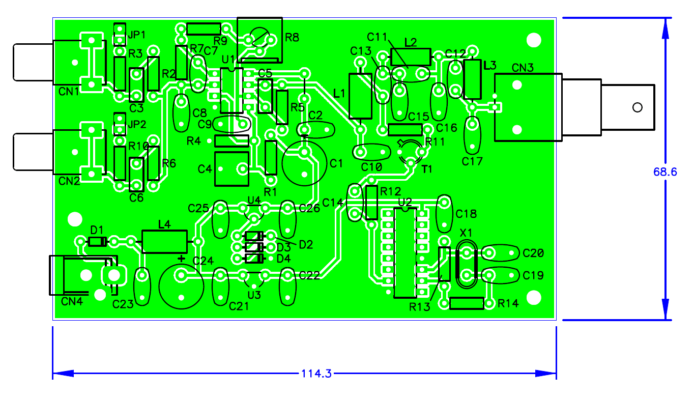
For those who want to make the PCB, the layout is visible in the figure below. The exact dimensions are 114.3 x 68.6 mm2 and it's viewed from below (solder side).

For those who prefer to get the PCB professionally manufactured, I exported the Gerber files, ready to be sent to a fabricator. While I was at it, I included all layers for a double-sided PCB, as they often cost as much as a single sided one... but on the top side, there is only a single bridge. You can still decide to have just a single sided PCB by telling your fabricator to manufacture only the bottom layer.
The PCB Gerber files can be downloaded here: am-mod-pcb.zip (90,313 bytes).
The picture below shows the board completely assembled.
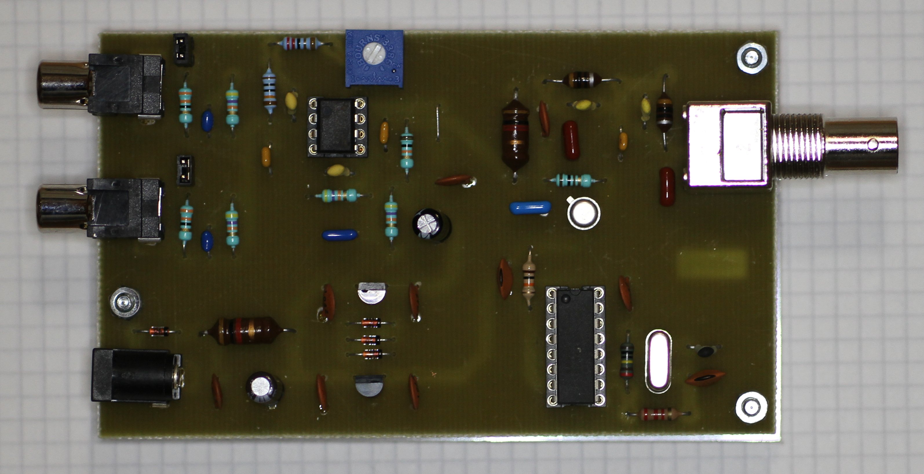
In spite of what one may think by looking at the picture at the beginning of this page, the modulator should be installed in a metallic box to shield it and preventing the radio from picking up noise generated from U2.
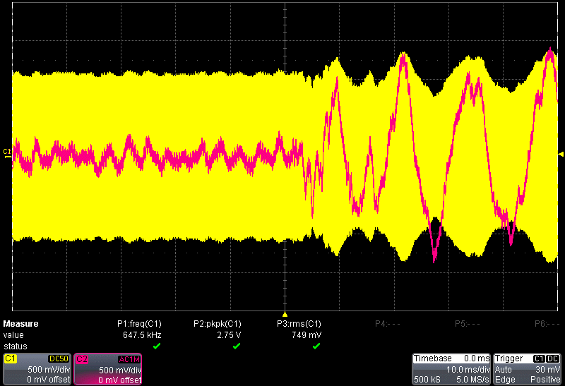
When the board is finally assembled, let's connect the power supply and switch the power on. As described earlier, it should use about 40 mA at 12 V. Let's first check if the oscillator works by connecting an oscilloscope to the oscillator buffered output (U2, pin 9). A square signal with TTL levels (0 to 5 V) at the crystal frequency should be clearly visible (10.368 MHz in this case). This signal is visible in the figure below (CH2, pink). One could also view the signal on the oscillator amplifier output (U2, pin 10), but in this case a low capacitance high impedance (10x) probe should be used to avoid loading the oscillator circuit.
On the same figure, one can also see the board output signal (with no modulation), where the frequency has been divided by 16 by U2 (648 kHz in this case) and the square wave has been filtered out to sinusoidal wave by the output filter (CH1, yellow). The output must be connected on a 50 Ω load; many oscilloscopes can switch their input impedance to 50 Ω, otherwise an external resistor must be used. The amplitude is 2 Vpp (0.7 Vrms, +10 dBm), as expected.

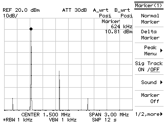
Now, let's have a look at the output spectrum. Since the power is low, the output can be directly connected to the spectrum analyzer input without taking the risk of damaging it (most spectrum analyzers can survive powers of +20 to +30 dBm). On the other hand, you may want to activate the attenuator function (30 dB in this case) to avoid the analyzer to saturate and give inaccurate results. The spectrum analyzer already has in input impedance of 50 Ohms, so there is no need to bother with an external load. The output spectrum is visible in the figure below. The spectrum analyzer agrees with the previous measurement taken with the oscilloscope and finds a carrier power of +10.8 dBm. The second and third harmonics are clearly visible and their power are –26 dBm (2.5 μW, 36 dB below the carrier) and –50 dBm (10 nW, 60 dB below the carrier). These harmonic levels are fine for a simple modulator that is not supposed to be used as a transmitter.
Now, let's add the modulation. For this, a CD or MP3 player has to be connected to CN1 and CN2. JP1 and JP2 are set according to the required impedance of the audio source. The oscilloscope is connected at the board output which is loaded with 50 Ω. This signal is visible in the figure below (CH1, yellow). To have a comparison, the audio signal is measured as well (CH2, pink) and to take advantage of the additionner circuit, it was measured on U1:A's, pin 1. The AM modulation is clearly visible.
Then, R8 has to be adjusted to the highest possible modulation factor without clipping (distorting) the signal. It's not easy to find the best possible adjustment because CD players have a very high dynamic range and some songs may produce very high audio peaks. It's safer to adjust R8 to a lower modulation factor: even if the factor is 70 or 80 %, the modulated audio level will be enough and for this application we don't care about power efficiency. If the modulation is adjusted too low, one will have to increase the volume on the connected radio.
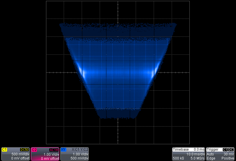
The figure below shows the linearity of this modulator. On the horizontal (X) axis is the modulated RF signal at the output of the board, on the vertical (Y) is the audio signal at the modulation amplifier output (U1:B, pin 7). The nice symmetric trapezoid shape shows a good linearity. If this wasn't the case the two tilted sides were curved. It the modulation factor is increased, the trapezoid becomes a triangle (100 % modulation) and a triangle plus a line (over-modulation). In this case the modulation factor is safely below 100 %.
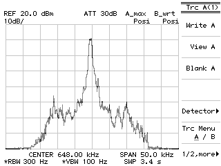
Finally, let's have a look at the sidebands with the spectrum analyzer. The board output is connected directly to the spectrum analyzer, the center frequency is set to match the carrier frequency and the span is set to 50 kHz. Receiver and video bandwidth are set as small as possible (300 and 100 Hz respectively in this case) and the display is set in peak-hold mode, since reducing the bandwidth dramatically slows down the analyzer and one has to accumulate a lot of sweeps to see the final shape. So, the measure is taken for several minutes while modulating with some music. The result is in the figure below: the carrier is visible in the center and the sidebands are symmetrical to it. The modulation is wider than the expected 9 kHz, because the low-pass filters in U1 only have a total attenuation of 20 dB/decade, but again, this spectrum is fine if it's not intended to be transmitted.
The first solution one would think about is connecting the output of the modulator to the antenna connector of the radio with a suitable attenuator. But this solution could be very dangerous because old radios often do not have a ground connection and the insulation almost half a century old may be not as effective as it should. An electrical shock may result. There is the risk of having mains potential on the radio chassis. The situation can be even worse, because cheap vintage radios often use an autotransformer instead of an isolated transformer and the chassis is physically connected to one of the AC mains line wires. This can be very dangerous because the mains potential would also reach our modulator and the MP3 player via the antenna and audio cables. For these reasons this solution is not recommended. Use it only if you know what you are doing and that you are sure about the quality of the ground connection of your radio, and of course at your own risk.
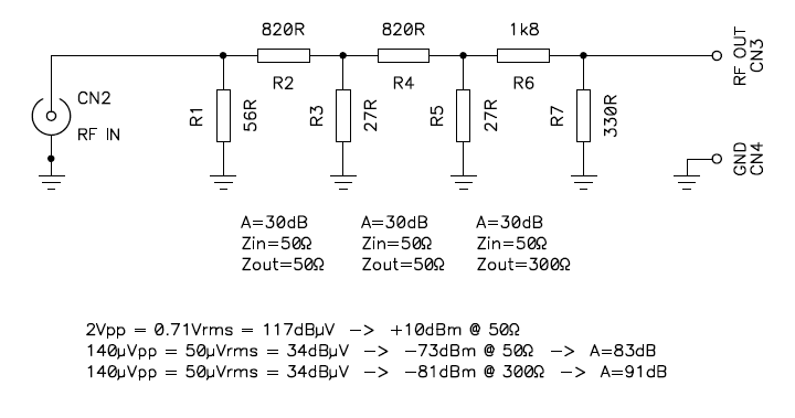
On the other hand, for more recent radios, connecting the RF output of the modulator to the antenna input of the receiver via a suitable attenuator is definitively the best solution, and for this reasons this solution is discussed anyway. If we consider that a S9 signal strength (50 μV) represents –73 dBm (on 50 Ω) and that the power available at the output of the modulator is +10 dBm, we have to attenuate 83 dB. Old radios usually have an input impedance of 300 Ω, therefore an S9 signal would be –81 dBm and the attenuator should remove 91 dB. The exact value of the attenuator is not really e problem, since the signal strength will be compensated bay the automatic gain control of the radio. We just want to avoid a too strong signal that may introduce distortion and a too weak signal that would introduce noise. Any attenuator in the 80 to 90 dB range will do the job. The one shown in the figure below attenuate 90 dB and also converts the impedance from 50 Ω to 300 Ω.
If one would like to add some extra security, the attenuator could be connected to the radio via two 10 nF 1 kV capacitors, in order to limit a possible AC mains current due to bad isolation. But in any case, this solution is not recommended for connecting to a vintage radio.
A much safer way to connect the modulator to the radio is via an inductive coupling: in this way there is no direct connection to the radio circuit and there is no risk of electrical shock in case of bad radio insulation.
The basic idea is to connect the output of the modulator to a coil and put this coil in close vicinity of the receiver antenna tuned circuit, in order to make a transformer between the two coils. Wooden radios are usually not (or very badly) shielded, so the coupling coil can be outside the radio and no connection nor modification is required.
The simplest coil one could build is something like 8 turns of thin insulated wire over a diameter of about 110 mm and connect it directly to the modulator output via a coaxial cable. Coil dimensions and geometry are far form being critical. Than, one has to try to get the best coupling by moving the coil position and orientation near the radio. Depending on the model, the coil could be on the back, below, or close to one side of the radio. Usually the antenna tuner circuit is located in close proximity of the band switch, if the receiver has one.
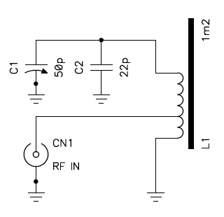
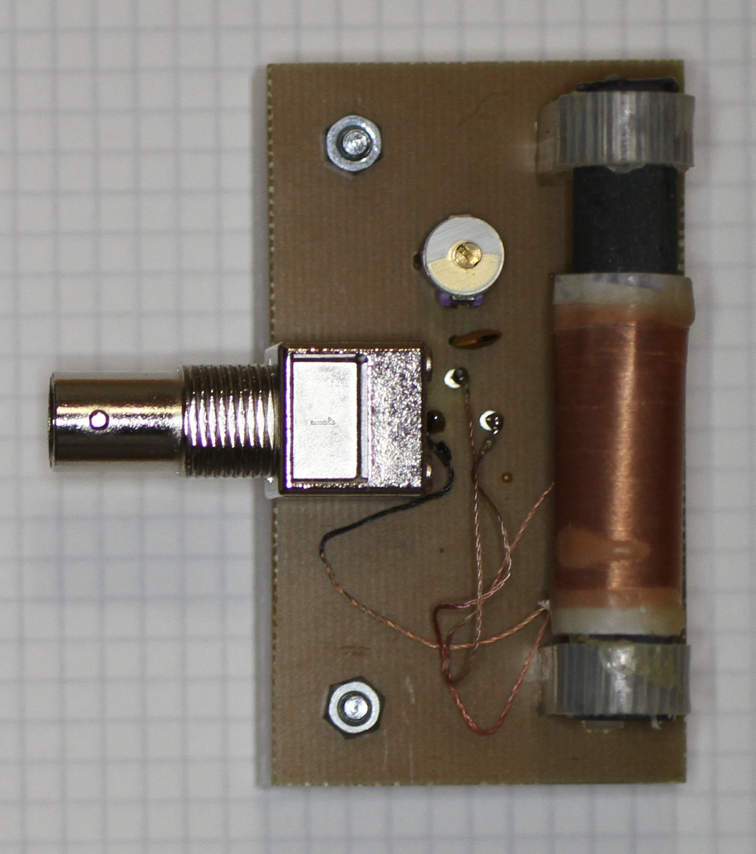
A more elaborated coil can be made using e ferrite rod antenna that are usually found in old transistor radios. It's easy to make a resonant circuit and increase the desired signal. The nice thing is that there are big chances that in the broken transistor radio from where the ferrite antenna comes from, there is the variable capacitor needed to resonate it into the MW band. If not, as it was the case with the rod in the figure below, one has to find another (variable) capacitor to do the job. Of course the values of the capacitors depend on the kind of rod antenna used.
Moving the coupling coil only a meter or so away from the radio makes the signal completely disappear, showing that we have really a "transformer" type coupling and that the RF energy is not radiated by the coupling coil in the form of an electromagnetic wave. So we are now sure that this is not a transmitter and that we are not radiating any signal in the MW band.
In this page a simple AM modulator for the MW band has been described. It allows listening to some musing on vintage radios even if the local broadcast transmitter has been switched off. The results were quite good and the same circuit can be used as test modulator for repairing AM receivers.
| Home | Electronics | Page hits: 119829 | Created: 02.2011 | Last update: 10.2021 |